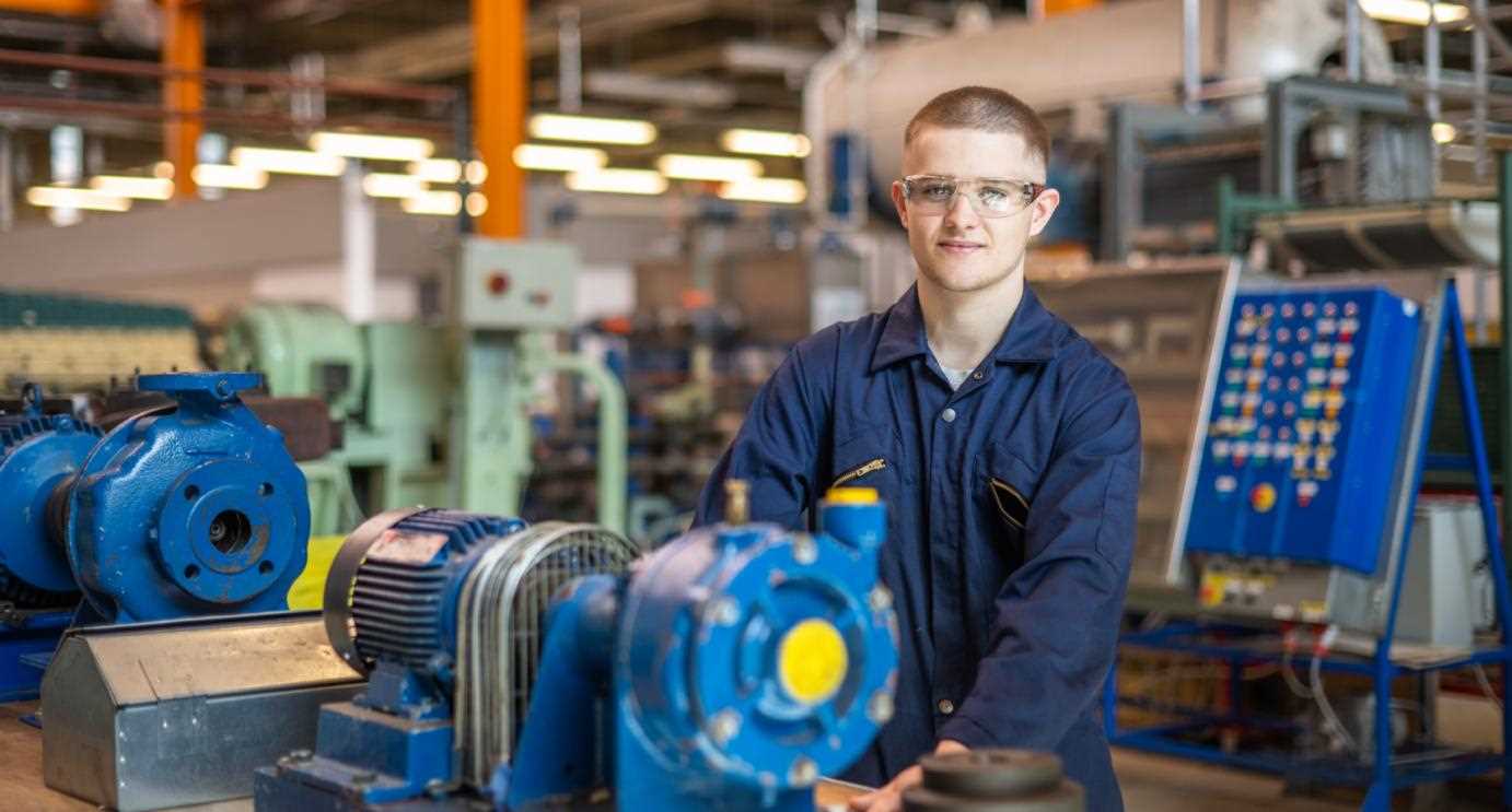
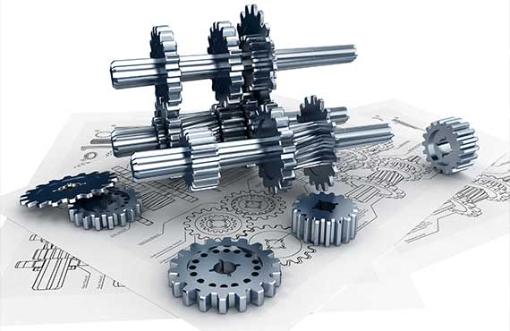
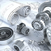
Concept Design
The first step in our process involves working closely with you to understand your product requirements and visualize the overall system.
We create a detailed process that includes mockups,
and CAD schematic and layout modeling to identify the ideal component placement and routing.
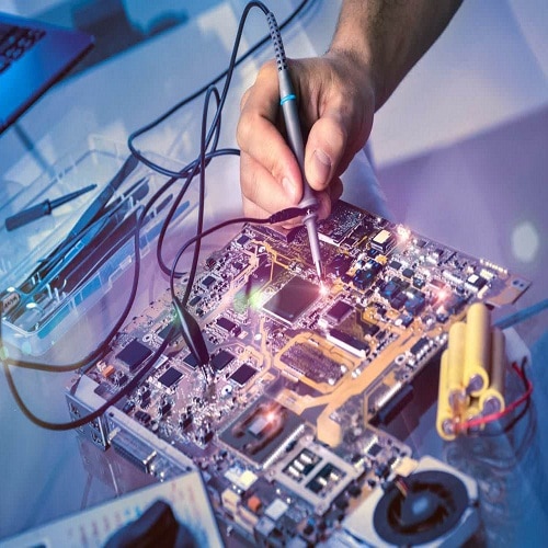
PCB Detail Design
Based on the concept design, we begin the detailed layout and design of the custom board.
We take into consideration component placement, trace routing, layer stackup, thermal management,
and other factors to guarantee the PCB functions perfectly within the overall system. Throughout this design phase,
we maintain close collaboration with you to gather your feedback and ensure the PCB meets your specific requirements.
PCB Development
PCB Prototyping
To validate the PCB design, we use our rapid prototyping capabilities.
This allows us to quickly create physical quick turn PCB and integrate them with the mechanical enclosure and other system components.
These prototypes enable us to test the design, identify issues, and make necessary adjustments before manufacturing.
We will then be able to incorporate your valuable input into the final design.
PCB Development
Validation and Testing
After integrating the PCB into the system, we conduct rigorous Engineering Validation Testing (EVT) in collaboration with external labs. This process ensures the design meets all functional requirements and regulatory standards. We also assist you in obtaining essential certifications such as FCC, UL, and CE, which guarantee features like reduced interference and improved safety for your users. We further provide support in supervised focus groups and quality assurance testing, ensuring your product meets the highest standards of user satisfaction.
PCB Development
Production-Ready Design
Following a successful EVT, we initiate the Design Validation Testing (DVT) phase. Our goal, at SDS, is to develop a product that mirrors the final production design. We collaborate closely with your contract manufacturer (CM), addressing any issues that arise and adjusting the manufacturing process. Following the completion of the Design Verification Testing (DVT) phase, we can proceed to Production Validation Testing (PVT), increase production, and full-scale manufacturing, with our team offering ongoing support to ensure a seamless transition. Throughout the entire custom PCB development process, our experts apply their deep knowledge in diverse specialist areas to deliver highly integrated, high-performance solutions that meet your specific needs and exceed user expectations.